Tiny crystal “seeds” could solve a hidden flaw in perovskite solar cells—unlocking high efficiency at larger scales.
Traditional perovskite solar cells (PSCs) are built with the electron transport layer underneath the perovskite light-absorbing layer and the hole transport layer on top. While this design has delivered strong performance in laboratories, it faces challenges when scaled up for mass production and long-term stability.
Inverted PSCs flip that structure, placing the hole-transport layer beneath the perovskite and the electron-transport layer above it. This configuration offers strong power conversion potential and works well with scalable solution-based manufacturing methods, making it an attractive option for next-generation solar technology.
However, inverted PSCs have struggled with a persistent weakness. Their efficiency and durability are often limited by microscopic structural irregularities and electronic defects at the bottom interface, also known as the buried interface, where the perovskite layer meets the hole transport layer. Because this region is hidden within the device, it has been especially difficult to control with precision.
Crystal-Solvate Pre-Seeding Strategy
To tackle this issue, researchers at the Qingdao Institute of Bioenergy and Bioprocess Technology (QIBEBT) of the Chinese Academy of Sciences developed a crystal-solvate (CSV) pre-seeding approach designed to carefully manage this critical bottom interface. Their method opens the door to producing high-efficiency, large-area perovskite solar modules. The findings were published today (February 27) in Nature Synthesis.
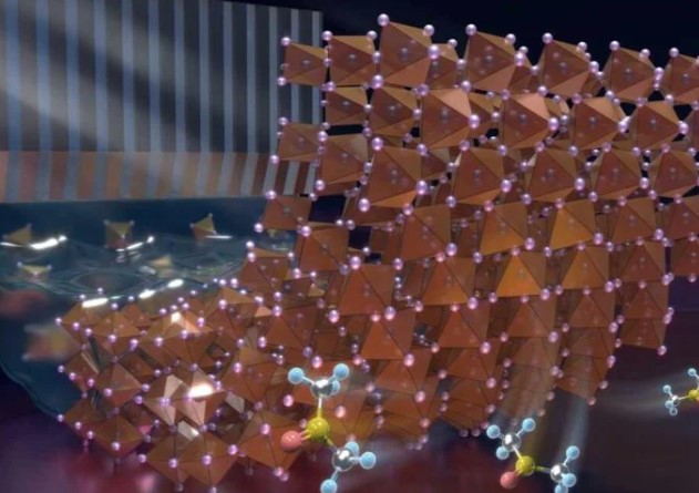
The technique begins by depositing specially engineered low-dimensional halide crystal-solvate seeds with the chemical formula PDPbI4·DMSO onto self-assembled monolayer (SAM)-modified substrates. These CSV nanocrystals act as a structural guide for the perovskite layer that forms afterward.
The rod-shaped CSV nanocrystals improve how well the perovskite precursor solution spreads across the typically water-repelling SAM surface. This ensures even coverage. As the perovskite crystals begin to form, the pre-seeded nanocrystals serve as plentiful nucleation sites, helping the crystals grow more quickly and in a more organized way.
Lattice-Confined Solvent Annealing
A key feature of the method involves dimethyl sulfoxide (DMSO) molecules that are built into the CSV crystal structure. When the material is heated during thermal annealing, these DMSO molecules are gradually released. This creates what the team describes as a “lattice-confined solvent annealing” environment at the bottom interface.


comments


Other categories
Recent Comments